TECHNOTE LT03-0020
Capacitive Sensor TechNote LT03-0020
Copyright © 2012 Lion Precision. www.lionprecision.com
Summary
This TechNote reviews concepts and theory of capacitive sensors to help in optimizing capacitive sensor performance. It also defines capacitive sensor terms as used throughout Lion Precision literature and manuals.
Lion Precision capacitive sensor products can be found here.
The TechNote is organized as such:
- Capacitance and Distance
- Focusing the Electric Field
- Effects of Target Size
- Range of Measurement
- Multiple Channel Sensing
- Effects of Target Material
- Measuring Non-Conductors
- Maximizing Accuracy
- Maximizing Accuracy: Target Size
- Maximizing Accuracy: Target Shape
- Maximizing Accuracy: Surface Finish
- Maximizing Accuracy: Parallelism
- Maximizing Accuracy: Environment
- Factory Calibration
- Sensitivity
- Sensitivity Error
- Offset Error
- Linearity Error
- Error Band
- Bandwidth
- Resolution
Capacitance and Distance
Non-contact capacitive sensors work by measuring changes in an electrical property called capacitance. Capacitance describes how two conductive objects with a space between them respond to a voltage difference applied to them. When a voltage is applied to the conductors, an electric field is created between them causing positive and negative charges to collect on each object (Fig. 1). If the polarity of the voltage is reversed, the charges will also reverse.
Capacitive sensors use an alternating voltage which causes the charges to continually reverse their positions. The moving of the charges creates an alternating electric current which is detected by the sensor (Fig. 2). The amount of current flow is determined by the capacitance, and the capacitance is determined by the area and proximity of the conductive objects. Larger and closer objects cause greater current than smaller and more distant objects. The capacitance is also affected by the type of non-conductive material in the gap between the objects.
Technically speaking, the capacitance is directly proportional to the surface area of the objects and the dielectric constant of the material between them, and inversely proportional to the distance between them (Fig. 3).
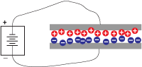 Figure 1 |
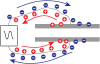 Figure 2 |
 Figure 3 |
In typical capacitive sensing applications, the probe or sensor is one of the conductive objects; the target object is the other. (Using capacitive sensors to sense plastics and other insulators is discussed in the nonconductive targets section.) The sizes of the sensor and the target are assumed to be constant as is the material between them. Therefore, any change in capacitance is a result of a change in the distance between the probe and the target. The electronics are calibrated to generate specific voltage changes for corresponding changes in capacitance. These voltages are scaled to represent specific changes in distance. The amount of voltage change for a given amount of distance change is called the sensitivity. A common sensitivity setting is 1.0V/100µm. That means that for every 100µm change in distance, the output voltage changes exactly 1.0V. With this calibration, a +2V change in the output means that the target has moved 200µm closer to the probe.
Focusing the Electric Field
When a voltage is applied to a conductor, the electric field emanates from every surface. In a capacitive sensor, the sensing voltage is applied to the Sensing Area of the probe (Figs. 4, 5).
For accurate measurements, the electric field from the sensing area needs to be contained within the space between the probe and the target. If the electric field is allowed to spread to other items or other areas on the target then a change in the position of the other item will be measured as a change in the position of the target.
A technique called “guarding is used to prevent this from happening. To create a guard, the back and sides of the sensing area are surrounded by another conductor that is kept at the same voltage as the sensing area itself (Fig. 4, 6).
When the voltage is applied to the sensing area, a separate circuit applies the exact same voltage to the guard. Because there is no difference in voltage between the sensing area and the guard, there is no electric field between them. Any other conductors beside or behind the probe form an electric field with the guard instead of the sensing area. Only the unguarded front of the sensing area is allowed to form an electric field with the target.
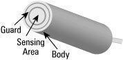 Figure 4 Capacitive sensor probe components |
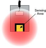 Figure 5 |
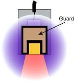 Figure 6 |
Effects of Target Size
The target size is a primary consideration when selecting a probe for a specific application. When the sensing electric field is focused by guarding, it creates a slightly conical field that is a projection of the sensing area. The minimum target diameter for standard calibration is 130% of the diameter of the sensing area. The further the probe is from the target, the larger the minimum target size.
Range of Measurement
The range in which a probe is useful is a function of the size of the sensing area. The greater the area, the larger the range. The driver electronics are designed for a certain amount of capacitance at the probe. Therefore, a smaller probe must be considerably closer to the target to achieve the desired amount of capacitance. The electronics are adjustable during calibration but there is a limit to the range of adjustment.
In general, the maximum gap at which a probe is useful is approximately 40% of the sensing area diameter. Standard calibrations usually keep the gap considerably less than that.
Multiple Channel Sensing
Frequently, a target is measured simultaneously by multiple probes. Because the system measures a changing electric field, the excitation voltage for each probe must be synchronized or the probes would interfere with each other. If they were not synchronized, one probe would be trying to increase the electric field while another was trying to decrease it thereby giving a false reading.
Driver electronics can be configured as masters or slaves. The master sets the synchronization for the slaves in multiple channel systems.
Effects of Target Material
The sensing electric field is seeking a conductive surface. Provided that the target is a conductor, capacitive sensors are not affected by the specific target material. Because the sensing electric field stops at the surface of the conductor, target thickness does not affect the measurement. .
Measuring Non-Conductors
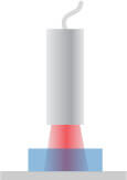
Figure 7
Non-conductors can be measured by passing the electric field through them to a stationary conductive target behind.
Capacitive sensors are most often used to measure the change in position of a conductive target. But capacitive sensors can be effective in measuring presence, density, thickness, and location of non-conductors as well. Non-conductive materials like plastic have a different dielectric constant than air. The dielectric constant determines how a non-conductive material affects capacitance between two conductors. When a non-conductor is inserted between the probe and a stationary reference target, the sensing field passes through the material to the grounded target (Fig. 7). The presence of the non-conductive material changes the dielectric and therefore changes the capacitance. The capacitance will change in relation to the thickness or density of the material.
Maximizing Accuracy
Now that we’ve discussed the basics of how capacitive sensing works, we can form strategies for maximizing effectiveness and minimizing error when capacitive sensors are used. Accuracy requires that the measurements be made under the same conditions in which the sensor was calibrated. Whether it’s a sensor calibrated at the factory or one that is calibrated during use, repeatable results come from repeatable conditions. If we only want distance to affect the measurement, then all the other variables must be constant. The following sections discuss common error sources and how to minimize them.
Maximizing Accuracy: Target Size
Figure 9
An undersized target causes the sensing field to extend to the sides of the target, introducing error
Unless otherwise specified, factory calibrations are done with a flat conductive target that is considerably larger than the sensing area. A sensor calibrated in this way will give accurate results when measuring a flat target more than 30% larger than the sensing area. If the target area is too small, the electric field will begin to wrap around the sides of the target meaning the electric field extends farther than it did in calibration and will measure the target as farther away (Fig. 9). In this case, the probe must be closer to the target for the same zero point. Because this distance differs from the original calibration, error will be introduced. Error is also created because the probe is no longer measuring a flat surface.
If the distance between the probe and the target is considered the Z axis, then an additional problem of an undersized target is that the sensor becomes sensitive to X and Y location of the probe. Without changing the gap, the output will change significantly if the probe is moved in either the X or Y axis because less of the electric field is going to the center of the target and more is going around to the sides.
Maximizing Accuracy: Target Shape
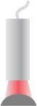
Figure 10 A curved target will require that the probe be closer and the sensitivity will be affected
Shape is also a consideration. Because the probes are calibrated to a flat target, measuring a target with a curved surface will cause errors (Fig. 10). Because the probe will measure the average distance to the target, the gap at zero volts will be different than when the system was calibrated. Errors will also be introduced because of the different behavior of the electric field with the curved surface. In cases where a non-flat target must be measured, the system can be factory calibrated to the final target shape. Alternatively, when flat calibrations are used with curved surfaces, multipliers can be provided to correct the measurement value.
Maximizing Accuracy: Surface Finish
When the target surface is not perfectly smooth, the system will average over the area covered by the spot size of the sensor. The measurement value can change as the probe is moved across the surface due to a change in the average location of the surface. The magnitude of this error depends on the nature and symmetry of the surface irregularities.
Maximizing Accuracy: Parallelism
During calibration the surface of the sensor is parallel to the target surface. If the probe or target is tilted any significant amount, the shape of the spot where the field hits the target elongates and changes the interaction of the field with the target. Because of the different behavior of the electric field, measurement errors will be introduced. At high resolutions, even a few degrees can introduce error. Parallelism must be considered when designing a fixture for the measurement.
Maximizing Accuracy: Environment
Lion Precision capacitive sensor systems are compensated to minimize drift due to temperature from 22°C – 35°C (72°F – 95°F). In this temperature range, errors are less than 0.5% of full scale.
A more troublesome problem is that virtually all materials used in targets and fixtures exhibit a significant expansion and contraction over this temperature range. When this happens, the temperature-related changes in the measurement are not gauge errors. They are real changes in the gap between the target and the probe. Careful fixture design goes a long way toward minimizing this error and maximizing accuracy.
The dielectric constant of air is affected by humidity. As humidity increases the dielectric constant increases. Humidity can also interact with probe construction materials. Experimental data shows that changes from 50%RH to 80%RH can cause errors up to 0.5% of full scale.
While Lion Precision probe materials are selected to minimize these errors, in applications requiring utmost precision, control of temperature and humidity is standard practice. International standards specify that measurements shall be done at 20°C or corrected to “true length” at 20°C.
Factory Calibration
Lion Precision’s capacitive sensor calibration system was designed in cooperation with Professional Instruments, a world leader in air bearing spindle and slide design. Its state-of-the-art design is driven by precision motion control electronics with positional accuracies of less than 0.012µm uncertainty.
The calibration system is certified on a regular basis with a NIST traceable laser interferometer. The measurement equipment used during calibration (digital meters and signal generators) are also calibrated to NIST traceable standards. The calibration information for each of these pieces of equipment is kept on file for verification of traceability.
Technicians use the calibration system to precisely position a calibration target at known distances to the capacitive sensor. The measurements at these points are collected and the sensitivity and linearity are analyzed by the calibration system. The analysis of the data is used to adjust the system being calibrated to meet order specifications.
After sensitivity and linearity are calibrated, the capacitive sensor systems are placed in an environmental chamber where the temperature compensation circuitry is calibrated to minimize drift over the temperature range of 22°C to 35°C. Measurements are also taken of bandwidth and output noise which affect resolution.
When calibration is complete, a calibration certificate is generated. This certificate is shipped with the ordered system and archived. Calibration certificates conform to section 4.8 of ISO 10012-1.
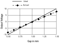
Sensitivity
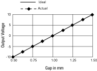
Sensitivity – The slope of the line is the sensitivity; in this case 1V/0.05mm.
Sensitivity indicates how much the output voltage changes as a result of a change in the gap between the target and the capacitive sensor. A common sensitivity is 1V/0.1mm. This means that for every 0.1mm of change in the gap, the output voltage will change 1V. When the output voltage is plotted against the gap size, the slope of the line is the sensitivity.
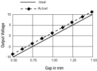
Sensitivity Error
Sensitivity Error – The slope of the actual measurements deviates from the ideal slope.
A sensor’s sensitivity is set during calibration. When sensitivity deviates from the ideal value this is called sensitivity error, gain error, or scaling error. Since sensitivity is the slope of a line, sensitivity error is usually presented as a percentage of slope; comparing the ideal slope with the actual slope.
Offset Error
Offset error occurs when a constant value is added to
Offset Error – A constant value is added to all measurements.
the output voltage of the system. Capacitive sensor systems are usually “zeroed” during setup, eliminating any offset deviations from the original calibration. However, should the offset error change after the system is zeroed, error will be introduced into the measurement. Temperature change is the primary factor in offset error. Lion Precision systems are compensated for temperature related offset errors to keep them less than 0.04%F.S./°C.
Linearity Error
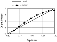
Linearity Error – Measurement data is not on a straight line.
Sensitivity can vary slightly between any two points of data. This variation is called linearity error. The linearity specification is the measurement of how far the output varies from a straight line.
To calculate the linearity error, calibration data is compared to the straight line that would best fit the points. This straight reference line is calculated from the calibration data using a technique called least squares fitting. The amount of error at the point on the calibration curve that is furthest away from this ideal line is the linearity error. Linearity error is usually expressed in terms of percent of full scale. If the error at the worst point was 0.001mm and the full scale range of the calibration was 1mm, the linearity error would be 0.1%.
Note that linearity error does not account for errors in sensitivity. It is only a measure of the straightness of the line and not the slope of the line. A system with gross sensitivity errors can be very linear.
Error Band
Error band accounts for the combination of linearity and sensitivity errors. It is the measurement of the worst case absolute error in the calibrated range. The error band is calculated by comparing the output voltages at specific gaps to their expected value. The worst case error from this comparison is listed as the system’s error band.
|
Gap |
Expected |
Actual |
Error |
| 0.50 | -10.000 | -9.800 | -0.010 |
| 0.75 | -5.000 | -4.900 | -0.005 |
| 1.00 | 0.000 | 0.000 | 0.000 |
| 1.25 | 5.000 | 5.000 | 0.000 |
| 1.50 | 10.000 | 10.100 | 0.005 |
Error Band – the worst case deviation of the measured values from the expected values in a calibration chart. In this case, the error band is -0.010mm.
Bandwidth
Bandwidth is defined as the frequency at which the output falls to -3dB. This frequency is also called the cutoff frequency. A -3dB drop in the signal level equates to approximately 70% drop in actual output voltage. With a 15kHz bandwidth, a change of ±1V at low frequency will only produce a ±0.7V change at 15kHz. In addition to sensing high-frequency motion, fast responding outputs maximize phase margin when used in servo-control feedback systems. Some drivers provide selectable bandwidth for maximizing either resolution or response time.
Resolution
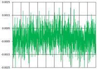
Figure 14
Noise from a 15kHz sensor
Resolution is defined as the smallest reliable measurement that a system can make. The resolution of a measurement system must be better than the final accuracy the measurement requires. If you need to know a measurement within 0.02µm, then the resolution of the measurement system must be better than 0.02µm.
The primary determining factor of resolution is electrical noise. Electrical noise appears in the output voltage causing small instantaneous errors in the output. Even when the probe/target gap is perfectly constant, the output voltage of the driver has some small but measurable amount of noise that would seem to indicate that the gap is changing. This noise is inherent in electronic components and can only be minimized, but never eliminated.
If a driver has an output noise of 0.002V with a sensitivity of 10V/1mm, then it has an output noise of 0.000,2mm (0.2µm). This means that at any instant in time, the output could have an error of 0.2µm.
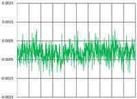
Figure 15
Noise from a 100Hz sensor
The amount of noise in the output is directly related to bandwidth. Generally speaking, noise is distributed uniformly over a wide range of frequencies. If the higher frequencies are filtered before the output, the result is less noise and better resolution (Figs. 14, 15). When examining resolution specifications, it is critical to know at what bandwidth the specifications apply. See our complete article on the relationships between resolution and bandwidth and how to be sure you’re getting accurate information from datasheets.