Application Note LA05-0010
Copyright © 2009 Lion Precision. www.lionprecision.com
Summary
Capacitive sensing technology can measure thickness of nonconductive films such as paper or plastic. The process can be effective and straightforward for large changes in thickness; however, resolving thickness to microns requires controlling or compensating for error sources which are often present in a production environment. The essential problem is a capacitive sensor’s low sensitivity to changes in film thickness and high sensitivity to changes in the gap between the sensor and a conductive target. Using capacitive and eddy-current sensing technologies together can alleviate some of the error sources. Additional mechanical and computational techniques will be required to produce micron resolution of film thickness.
Basic Film Measurement With Capacitive Sensors
Nonconductor Measurement
Figure 1. Non-conductors can be measured by passing the electric field through them to a stationary conductive target behind
Capacitive sensors make measurements based on the capacitance between the probe sensing area and a grounded conductive surface. Typical capacitive sensing applications measure the change in capacitance as the target moves closer to or farther from the probe. But capacitance is also changed by changing the dielectric constant of the material in the gap between the probe and the grounded conductive surface (figure 1). Most films have a dielectric constant considerably higher than air; because of this, changes in thickness of a film between the probe and a conductive reference surface will cause changes in the capacitance and change the output voltage of the sensor. For reliable results, the gap between the probe and the reference surface must be held constant. Because sensitivity is much higher to movements of the conductive surface than to changes in film thickness, small changes in the gap will produce large errors in film thickness.
Sensitivity Considerations
Capacitive sensors with linear outputs will also provide linear outputs when measuring film thickness but with a greatly decreased sensitivity. A sensor that produces one volt of change for a few microns of change in position of a conductive target may only produce a few millivolts of change for a few microns of change in film thickness. One of the factors that determines sensitivity to film thickness is the dielectric constant of the material (ε). Sensitivity is higher with higher dielectric constants. The table below lists dielectric constants of some common materials:
|
Material |
Dielectric Constant (ε) |
| Air | 1 |
| Mylar | 3.1 |
| Neoprene | 6.7 |
| Polyethylene | 2.25 |
| Teflon | 2.1 |
Another important factor in the sensitivity to film thickness is the capacitive sensor’s calibrated range. The sensitivity of the capacitive sensor to changes in film thickness is inversely proportional to the range of the sensor. Higher sensitivity to film thickness change requires that the capacitive sensor have a very small range and be very close to the film. The chart below shows a typical relationship between capacitive sensor range and sensitivity to film thickness changes for two different dielectric constants.
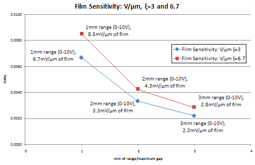
Film sensitivity relative to capacitive sensor range
Calibrating Sensitivity to Film Thickness
Capacitive sensors are generally calibrated for changes in position of a conductive target. Determining the sensitivity of a capacitive sensor to changes in film thickness requires two pieces of film of known thickness. Each piece is placed in the gap between the sensor and reference surface and measured; the difference between the two thicknesses and their respective measurements is the sensitivity of the system. Because the output is linear with respect to film thickness, this sensitivity should apply to all measurements within the range of the sensor.
Primary Production Error Sources
Metal Rollers
In a film production environment, most thickness measurements take place as the film is passing over a metal roller. The roller provides the required reference surface for the capacitive sensor, but the imperfect shape of the roller turning on imperfect bearings causes the roller to move toward and away from the capacitive probe as the roller turns (figure 2).
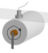
Figure 2. Imperfect rollers on imperfect bearings create a significant error source for the capacitive sensor
Scans
Many film applications need to scan the film thickness across the entire web. This is usually accomplished by moving the sensor across the web parallel to the roller. The mechanics of the scanning system are also imperfect and cause the roller-sensor gap to change during the scan (figure 3).
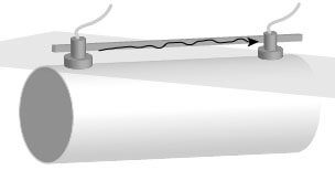
Figure 3. Imperfect scanner mechanics also create a significant error source for the capacitive sensor
Because the capacitive sensor is much more sensitive to movements of the conductive target, changes in film thickness are lost in these changes of the gap between the roller and the sensor.
Eddy-Current Sensors Solve Roller and Scan Problems
An eddy-current sensor cannot detect film or any other nonconductor. An eddy-current sensor can be used to monitor changes in the gap between the roller and the capacitive sensor. The gap changes measured by the eddy-current sensor can be subtracted from the changes measured by the capacitive sensor resulting in measurements of the film thickness only (figure 4).
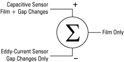
Differential measurement with capacitive and eddy-current sensors removes gap change errors from the system
Imperfect Sensors
If capacitive and eddy-current sensors were ideal, then the dual-technology film thickness sensor would be an ideal solution and film thickness measurement would be simplified. Because of the capacitive sensor’s relatively low sensitivity to film thickness changes, small errors that are usually insignificant in the capacitive and eddy-current sensors become significant factors in the measurement of film thickness. To use a dual-technology sensor solution to film thickness measurement, the error sources for the capacitive and eddy-current sensors must be controlled to a level smaller than the minimum film thickness resolution required. If the application requires measurement of 2µm changes in film thickness which is represented by 10mV, then the error sources must be significantly less than 10mV. There are several error sources common to noncontact sensing that will be important considerations. Each of them is discussed below.
Sensor Error Sources
Sensor error sources have the potential of being larger than the sensors’ sensitivity to small changes in film thickness. When using a dual-technology system, errors can double in magnitude if the polarity of the error is different for the capacitive and eddy-current sensors.
Linearity Error
All displacement sensors exhibit a small linearity error. Linearity errors occur when the sensitivity between measurement points is inconsistent over the range of the sensor. A common linearity error specification for capacitive and eddy-currents sensors is ±0.2% of full-scale range. In a worst-case scenario, the capacitive and eddy-current sensors would have opposite polarity linearity errors at the same point of their respective ranges. That would result in a combined error of 0.4% full scale. For a 0-10V output, the error voltage at that point would be 40mV. Referring to the Relative Error Magnitude chart at the end of this section, 40mV would be roughly equal to a 5µm error in film thickness for the most sensitive range listed in the chart, and a 20µm error for the least sensitive (widest gap) calibration. This system as is could not reliably measure 1 or 2µm changes in film thickness. “Mastering” the system can greatly reduce this error. We will discuss mastering after we discuss thermal drift.
Thermal Drift
All displacement sensors exhibit a small thermal drift. Changes in temperature cause mechanical changes in the probe structure and electrical drift in some of the electronic components. These are usually quite small, but with the low sensitivities involved with film thickness measurement, they can be significant. Thermal drift is primarily a DC shift in the output. The sensitivity (gain) can be affected, but that effect is much smaller than the DC shift. A typical thermal drift specification for capacitive and eddy-current sensors is ±0.04% Full-Scale/°C. When using two sensors, it is possible that their respective thermal drifts will be opposite which doubles the potential error to 0.08% Full-Scale/°C. For a change of 3°C, the output could change 24mV; this is equivalent to 3µm of film thickness for the most sensitive range, and over 10µm for the least sensitive range.
Mastering to Reduce Errors
Most of the errors created in a dual-technology film thickness measurement result from the differences in errors between the two sensors. If the two sensors’ errors could be matched, then the errors would be reduced to nearly zero when the measurements are combined mathematically. This can be accomplished by a process called “mastering.” Mastering involves the occasional testing and compensation of sensor performance during production. This can be done manually, but is usually an automated part of a computer controlled system.
Mastering to Reduce Linearity Errors
Reducing linearity errors (or any other sensitivity errors) involves moving the sensors off of the film and calibrating them as the gap between the roller and the sensors is changed. This can be accomplished with a mechanism that moves the sensors up and down or a multiple height target can be moved into multiple positions under the sensors. Data is collected from each sensor for the different gaps. Using a look-up table or by calculating polynomials, both sensors are calibrated mathematically to produce identical results at different gaps. Because linearity and sensitivity are not as susceptible to changes, the mastering process does not need to be frequent.
Mastering to Reduce Thermal Drift Errors
Reducing thermal errors only requires moving sensors off of the film to measure the roller with no film present. While off the film, the outputs of the sensors are mathematically set to zero and measurement resumes. If any thermal drift occurs, it is removed by resetting both sensors to zero when off the film. The frequency of this operation will be determined by the thermal environment of the installation and the thermal stability of the sensors. Frequent and/or large changes in temperature will require more frequent mastering.
Sensor Electrical Noise
All electrical devices, including sensors, produce a small amount of electrical noise in the output. As with other error sources, this noise is quite small but can become significant when measuring small changes (microns) in film thickness. Electrical noise is distributed over a large spectrum of frequencies. For this reason, a low-pass filter or low-bandwidth sensor can remove some of the noise and thereby reduce this error source. Actual resolution values are dependent on specific sensors and calibration, but typical values of noise for a capacitive sensor is 0.004% Full-Scale at 15kHz bandwidth, only 0.002% at 100Hz. With a 0-10V output, this is 0.2mV. Eddy-Current sensors have typical resolution values around 0.008% Full-Scale at 15kHz and 0.004% at 100Hz. With a 0-10V output, this is 0.4mV.
Relative Error Magnitude
The charts below shows the sensor’s voltage change for 1µm changes in film thickness and the error voltages possible in worst case scenarios for unmastered dual-technology sensing systems.
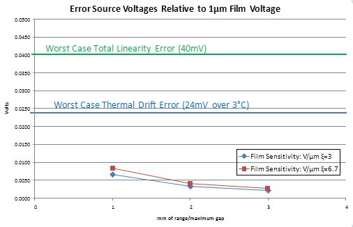
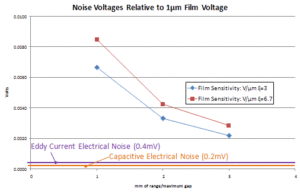
Magnitudes of film sensitivity and error sources are generalized approximations. Specific values will depend on final system configuration.
Sensor Target Areas
Using adjacent capacitive and eddy-current sensors may be effective, but differences in the location of the sensing areas will be an error source in the system. Changes in the gap between the capacitive sensor and conductive target will not match changes in the gap at the eddy-current sensor location; when film thickness resolution of microns is necessary, this error may be prohibitive. An ideal application of a dual-technology thickness system requires that the capacitive and eddy-current sensors measure the same location; this requires that the sensors be concentric. Specially designed dual-technology probes can make this possible.